 一、先進封裝市場持續強勁成長
根據Yole Développement的最新調查報告,全球先進封裝市場在2019年至2025年之間的複合年成長率(CAGR)為6.6%,預計將帶動市場營收在此期間增加一倍以上。Yole先進封裝團隊預測,到2025年該市場營收將突破420億美元。這幾乎是傳統封裝市場預期成長率(2.2%)的3倍。
Shacho San 發表在 痞客邦 留言(0) 人氣(156)
一、半絕緣碳化矽(SiC)發展現況
高頻用寬能隙半絕緣碳化矽晶圓具備高功率、耐高壓、耐高溫等特性,隨著毫米波通訊及5G相關產業起飛,受到世界各國政府與產業界的廣泛關注和高度重視,成為增長潛力巨大的戰略性產業。高頻/高功率放大器元件需具備SiC、GaN等寬能隙材料技術,將帶動另一波產業成長動能。其中半絕緣性SiC晶圓單價高昂且為戰略管制品,為各國亟需開發之關鍵基板材料。
1. SiC昇華生長現有技術
一般被稱為物理氣相傳輸(Physical Vapor Transportation; PVT)的昇華技術,已被廣泛地用於商業規模的SiC單晶之生長。不同於矽晶棒與藍寶石使用液相拉晶法在長晶過程中可隨時觀察晶體成長狀況,SiC氣相傳輸法是在高溫低壓及保護氣氛下於石墨坩堝中,將SiC料源昇華後一層一層如磊晶般,將碳矽原子堆疊於單晶晶種上,經過長達5~7天的時間,完成一SiC單晶晶球之生長。
Shacho San 發表在 痞客邦 留言(0) 人氣(544)
 一、EMI Shielding (電磁波屏蔽) 未來市場預估
5毫米波穿透力差,衰減大,覆蓋能力會大幅度減弱,因此5G對信號的抗干擾能力要求很高,需要大量的電磁屏蔽器件。
金屬材料雖具有良好的電磁屏蔽性能,但其密度大、易腐蝕等特點限制了其進一步應用,然而將金屬靶材做為5G SiP表面電磁波屏蔽或將會是更好的解決方案。
Shacho San 發表在 痞客邦 留言(0) 人氣(97)
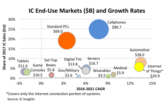
IC Insights’ IC Market Drivers 2018 report also projects good increases in IC sales for medical electronics, wearable systems, cellphones, servers, and gov/mil applications.
Integrated circuit sales for automotive systems and the Internet of Things are forecast to grow 70% faster than total IC revenues between 2016 and 2021, according to IC Insights’ new 2018 Integrated Circuit Market Drivers Report. ICs used in automobiles and other vehicles are forecast to generate worldwide sales of $42.9 billion in 2021 compared to $22.9 billion in 2016, while integrated circuit revenues for Internet of Things (IoT) functionality in a wide range of systems, sensors, and objects are expected to reach $34.2 billion in four years compared to $18.4 billion last year, says the new 358-page report.
Shacho San 發表在 痞客邦 留言(0) 人氣(14)
全球最大半導體代工企業台灣集成電路製造(簡稱台積電、TSMC)聯合首席執行官(CEO)劉德音12月7日表示,將向電路線寬為3奈米(奈米為10億分之1米)的新一代半導體投資超過200億美元。通過對尖端領域投入巨資,領先於韓國三星電子等競爭對手。
劉德音7日下午在台灣北部新竹發表演講時透露了上述消息。目前美國蘋果新款iPhone等配備的10奈米線寬半導體屬於最尖端產品。 7奈米產品將於2018年啟動量產,3奈米產品預計2022年量產。目前已具體落實3奈米產品項目的企業只有台積電。新工廠建在台南。
半導體大體上分為負責存儲的內存和負責運算的邏輯半導體。台積電的產品以邏輯半導體為主,目前多面向智能手機。該公司認為,2018年7奈米產品量產以後,在面向人工智能(AI)和數據中心方面的需求有望激增。
在半導體領域,縮小電路線寬成為降低成本和提高性能的關鍵。一方面,電路線寬的縮小導致生產難度提高,製造設備的價格正在暴漲。荷蘭半導體設備廠商阿斯麥(ASML)開發的「極紫外光刻(EUV光刻)」設備每台售價超過1億歐元。
Shacho San 發表在 痞客邦 留言(0) 人氣(5)

Silicon has provided enormous benefits to the power electronics industry. But performance of silicon-based power electronics is nearing maximum capacity.
Enter wide bandgap (WBG) semiconductors. Seen as significantly more energy-efficient, they have emerged as leading contenders in developing field-effect transistors (FETs) for next-generation power electronics. Such FET technology would benefit everything from power-grid distribution of renewable-energy sources to car and train engines.
Shacho San 發表在 痞客邦 留言(0) 人氣(4)
A group of spintronics researchers at EPFL is using new materials to reveal more of the many capabilities of electrons. The field of spintronics seeks to tap the quantum properties of “spin,” the term often used to describe one of the fundamental properties of elementary particles – in this case, electrons. This is among the most cutting-edge areas of research in electronics today.
Researchers working in the Laboratory of Nanoscale Electronics and Structures (LANES), which is run by Professor Andras Kis, were able to quantify these quantum properties for a category of two-dimensional semiconductors called transition metal dichalcogenides, or TMDCs. Their research projects, which were published recently in ACS Nano and today in Nature Communications, confirm that materials like graphene (C), molybdenite (MoS2) and tungsten diselenide (WSe2) offer, either alone or by combining some of their characteristics, new perspectives for the field of electronics – perspectives that could ultimately lead to smaller chips that generate less heat.
Shacho San 發表在 痞客邦 留言(0) 人氣(0)

The Semiconductor Industry Association (SIA) today announced worldwide sales of semiconductors reached $107.9 billion for the third quarter of 2017, marking the industry’s highest-ever quarterly sales and an increase of 10.2 percent compared to the previous quarter. Sales for the month of September 2017 were $36.0 billion, an increase of 22.2 percent over the September 2016 total of $29.4 billion and 2.8 percent more than the previous month’s total of $35.0 billion. All monthly sales numbers are compiled by the World Semiconductor Trade Statistics (WSTS) organization and represent a three-month moving average.
Shacho San 發表在 痞客邦 留言(0) 人氣(0)
在歷經冗長的3階段審查之後,11月下旬中國大陸官方終於有條件通過日月光與矽品合組產業控股公司,顯然全球半導體封測行業已進入整併潮,同時封測行業集團化時代儼然來臨。
而目前全球前10大封測廠已呈現3大陣營鼎立的情況,包括日月光與矽品、Amkor與J-Devices及Manium、長電科技與STATS ChipPAC等,而3大陣營若不含IDM廠,則台灣的市佔率將達到29%,領先第2大美國陣營的15%、第3大中國陣營的10%。
Shacho San 發表在 痞客邦 留言(0) 人氣(8)
A*STAR’s Institute of Microelectronics (IME) has established a development line to accelerate the development of fan-out wafer level packaging (FOWLP) capabilities for next-generation Internet of Things (IoT) technologies. The FOWLP development line, which is built upon existing infrastructure at IME’s facilities at Singapore Science Park II, and its new facilities at Fusionopolis Two, will allow IME and its partners (see Annex A for list of partners) to develop technologies that serve a wide range of markets such as that of consumer electronics, healthcare and automotive.
The IoT is set to become the next growth driver for the semiconductor industry, as demand for internet-connected devices continues to soar. FOWLP is an emerging breakthrough chip packaging technology platform aimed at meeting the technology requirements of next-generation electronic devices that require ultra- low power consumption rates, smaller package profiles, higher performance; and all made at a lower cost.
Shacho San 發表在 痞客邦 留言(0) 人氣(0)