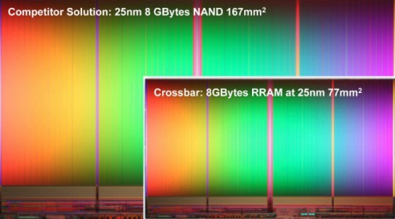
位於美國加州的創業公司Crossbar 發布了一種新型的芯片,能以郵票大小的體積存儲1TB 的數據。這種芯片採用RRAM 技術(可變電阻式記憶體,Resistive Random Access Memory),可顛覆傳統的閃速存儲器,數據存儲速度是其20 倍,很有可能成為每年600 億美元閃存市場的有力競爭者。
由於閃存是從iPhone 到平板電腦到數碼相機都必備的硬件之一,因此Crossbar 的前景被投資者看好,獲得了來自Kleiner Perkins Caufield & Byers,Artiman Ventures 和Northern Light Venture Capital 的2500 萬投資。
和閃存一樣,RRAM 也是一種非易失性的存儲器,這意味著數據可以永久儲存不丟失,哪怕是在電源被切斷的情況下。而Crossbar 在其設計中採用了三層結構的設計——一個非金屬底層電極,中間的無定形矽交換介質,還有最上層的金屬電極。當電壓施加至兩電極時,它交換介質內會形成一定數量的電阻細絲,因此其電阻式可變換的。
通過Crossbar 的芯片,未來手機和平板的存儲速度、備份、歸檔等各方面性能都將有所提升。而從企業角度出發,供應商可以在數據中心中搭建SSD 和雲計算設備。 RRAM 還可運用於物聯網中,甚至智能電錶、恆溫器這樣的智能設備,以及諸如Google Glass 等可穿戴式設備,因為它的電耗更低,可以延長電池使用壽命。
目前Crossbar 團隊有20 位成員,正準備自己製造芯片並向市場出售,同時也打算向system-on-a-chip 的供應商提供技術支持,在同個芯片中將RRAM 和其它組件聯繫到一起。 Crossbar 申請了100 項相關專利,其中30 項已被批獲。
IHS 的高級分析師Michael Yang 說:我們今天所存儲的90% 的數據都是近兩年產生的。實時的數據生成和接收越來越成為現代生活的一部分,並且在未來幾年還會快速增長。然而,我們過去一直沿用至今的存儲方式,比如二維的NAND(一種存儲技術),在物理和工程方面都顯露出巨大的局限性。而Crossbar 的RRAM 恰好邁過了這道門檻,因此很有可能成為未來取代性的存儲技術解決方案。
WORKING ARRAY VALIDATES MANUFACTURABILITY AND SIMPLICITY OF CROSSBAR RESISTIVE RAM
- Highest Capacity: Up to 1 Terabyte (TB) of Storage on a Single Chip; Multiple Terabytes with 3D Stacking
- Lowest Power: Extends Battery Life to Weeks, Months or Years
- Highest Performance: 20x Faster Write than NAND
- Easiest SOC Integration: Simple Stacking on Logic in Standard CMOS at Most Advanced Nodes
- Most Reliable: 10x the Endurance of NAND; Approaching DRAM Reliability

SANTA CLARA, CA – AUGUST 5, 2013 – Emerging from stealth-mode today, Crossbar, Inc., a start-up company pioneering a new category of very high capacity and high-performance non-volatile memory, unveiled its Crossbar Resistive RAM (RRAM) technology. This new generation of non-volatile memory will be capable of storing up to one terabyte (TB) of data on a single 200mm2 chip, enabling massive amounts of information, such as 250 hours of HD movies, to be stored and played back from an IC smaller than a postage stamp. Crossbar today also announced it has developed a working Crossbar memory array at a commercial fab, a major milestone in the development of new memory technology, signaling its readiness to begin the first phase of productization.
Due to its simple three-layer structure, Crossbar technology can be stacked in 3D, delivering multiple terabytes of storage on a single chip. Its simplicity, stackability and CMOS compatibility enable logic and memory to be easily integrated onto a single chip at the latest technology node, a capability not possible with other traditional or alternative non-volatile memory technologies.
“Non-volatile memory is ubiquitous today, as the storage technology at the heart of the over a trillion dollarelectronics market – from tablets and USB sticks to enterprise storage systems,” said George Minassian, chief executive officer, Crossbar, Inc. “And yet today’s non-volatile memory technologies are running out of steam, hitting significant barriers as they scale to smaller manufacturing processes. With our working Crossbar array, we have achieved all the major technical milestones that prove our RRAM technology is easy to manufacture and ready for commercialization. It’s a watershed moment for the non-volatile memory industry.”
Crossbar’s technology will deliver 20x faster write performance, 20x lower power consumption, and 10x the endurance at half the die size, compared to today’s best-in-class NAND Flash memory. With that breakthrough performance and reliability, very high capacity and low power consumption, Crossbar will enable a new wave of electronics innovation for consumer, enterprise, mobile, industrial and connected device applications.
Non-volatile memory is the most common storage technology used for both code storage (NOR) and data storage (NAND) in a wide range of electronics applications. According to market research firm Webfeet Research, non-volatile memory is expected to grow to become a $48.4 billion market in 2016. Crossbar plans to bring to market standalone chip solutions, optimized for both code and data storage, used in place of traditional NOR and NAND Flash memory. Crossbar also plans to license its technology to system on a chip (SOC) developers for integration into next-generation SOCs.
SAMPLE OF CROSSBAR TECHNOLOGY APPLICATIONS:
Consumer Electronics, Mobile Phones and Tablets – Stores all of your personal entertainment, data, photos and information in a device that fits in your pocket. Delivers very fast storage, playback, backup and archiving.
Enterprise Storage, SSDs and Cloud Computing – Extends SSD reliability and capacity. Improves performance for enterprise, data center and cloud storage systems.
The Internet of Things; The Industrial Internet – Delivers years of battery life for industrial and connected applications such as smart meters and thermostats. Wide temperature ranges allow for reliability in the extreme heat of the summer or freezing temperatures in the winter. Enables entirely new, highly integratedSOCs that can be powered with a button cell or energy harvesting from the environment such as solar, heat or simple vibrations.
Wearable Computing – Enables a new generation of wearable computing with high capacity storage in a very small, compact size with very low power consumption.
Secure Payments – Can permanently store the codes and encryption keys needed for secure applications such as large volume smart cards to high-end mobile processors for contactless payments.
WORKING MEMORY ARRAY UNDERSCORES SIMPLICITY; READINESS FOR COMMERCIALIZATION
The Crossbar memory cell is based on three simple layers: A non-metallic bottom electrode, an amorphous silicon switching medium and a metallic top electrode. The resistance switching mechanism is based on the formation of a filament in the switching material when a voltage is applied between the two electrodes. This simple and very scalable memory cell structure enables an entirely new class of RRAM, which can be easily incorporated into the back end of line of any standard CMOS manufacturing fab.
After completing the technology transfer to Crossbar’s R&D fab and technology analysis and optimization, Crossbar has now successfully developed its demonstration product in a commercial fab. This working silicon is a fully integrated monolithic CMOS controller and memory array chip. The company is currently completing the characterization and optimization of this device and plans to bring its first product to market in the embedded SOC market.
Source:http://www.crossbar-inc.com/events/press-releases/crossbar-emerges-from-stealth-mode.html


 留言列表
留言列表