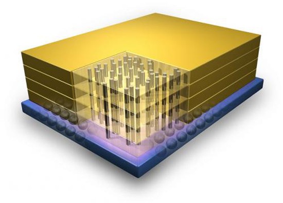
美國IBM與美光科技宣布,美光已決定利用基於矽通孔(Through-Silicon Via)的商用CMOS技術,率先生產新型存儲器“Hybrid Memory Cube”(HMC)(英文發布資料)。美光將利用IBM擁有的三維LSI製造工藝生產HMC,由此可將存儲器速度提高至現有產品的15倍左右。
美光的HMC通過TSV連接沿三維方向積層的多枚芯片。構成HMC的部件預定在IBM位於美國紐約州東菲什基爾(East Fishkill)的半導體工廠採用32nm級high-k金屬柵極工藝技術製造。採用TSV後,能夠以高效的數據傳輸速度連接高性能邏輯電路和最尖端的DRAM。 HMC試製品的每個LSI的最大數據傳輸速度為128GB/秒,與現有最尖端DRAM的12.8GB/秒相比,大幅提高了10倍。
另外,採用HMC可以大幅削減存儲器子系統的耗電量和封裝面積。據美光介紹,可在與原來保持同等數據傳輸速度的同時,將封裝面積和耗電量分別削減1/10和70%左右。
通過利用HMC,除了大規模網絡裝置、高性能計算系統和產業設備外,最終將應用於消費類產品,其功耗比也可大幅提高。
IBM院士(IBM Fellow)Subu Iyer發表了以下評論:“我們希望全面推廣的這個製造工藝,不僅是存儲器,還可向其他半導體產品提供具有優勢的解決方案。今後幾年內,三維芯片製造技術將會用於消費類產品中的半導體上。屆時,便攜終端的電池壽命和功能將會大幅改善”。
另外,美光DRAM營銷副總裁Robert Feurle表示,“HMC將給存儲器的使用方法帶來重大變革。設備設計人員可靈活地平衡存儲器系統耗電量與數據傳輸速度之間的關係。通過與IBM的合作,美光將提供業界最豐富的存儲器產品系列”。 (記者:大石 基之,《日經電子》)
IBM will present the details of its TSV manufacturing breakthrough at the IEEE International Electron Devices Meeting on December 5 in Washington, DC.
HMC parts will be manufactured at IBM's advanced semiconductor fab in East Fishkill, N.Y., using the company's 32nm, high-K metal gate process technology.
HMC technology uses advanced TSVs — vertical conduits that electrically connect a stack of individual chips — to combine high-performance logic with Micron's state-of-the-art DRAM. HMC delivers bandwidth and efficiencies a leap beyond current device capabilities. HMC prototypes, for example, clock in with bandwidth of 128 gigabytes per second (GB/s). By comparison, current state-of-the-art devices deliver 12.8 GB/s. HMC also requires 70 percent less energy to transfer data while offering a small form factor — just 10 percent of the footprint of conventional memory.
HMC will enable a new generation of performance in applications ranging from large-scale networking and high-performance computing, to industrial automation and, eventually, consumer products.
"This is a milestone in the industry move to 3D semiconductor manufacturing," said Subu Iyer, IBM Fellow. "The manufacturing process we are rolling out will have applications beyond memory, enabling other industry segments as well. In the next few years, 3D chip technology will make its way into consumer products, and we can expect to see drastic improvements in battery life and functionality of devices."
"HMC is a game changer, finally giving architects a flexible memory solution that scales bandwidth while addressing power efficiency," said Robert Feurle, Vice President of DRAM Marketing for Micron. "Through collaboration with IBM, Micron will provide the industry's most capable memory offering."
Provided by IBM
資料來源:http://www.physorg.com/news/2011-12-ibm-micron-hybrid-memory-cube.html


 留言列表
留言列表