
採用二硫化鉬(molybdenum disulfide)通道與單奈米碳管閘極的1奈米電晶體
(來源:Sujay Desai/UC Berkeley, Lawrence Berkeley National Laboratory)
碳奈米管從過去幾十年就已經用於製作實驗性電晶體,但大多是當做電晶體通道(channel);美國勞倫斯柏克萊國家實驗室(Lawrence Berkeley National Laboratory)的研究人員則是以奈米碳管製作閘極(gate),並因此實現了號稱全世界最小的電晶體。
該實驗室研究人員Ali Javey表示,以物理學規則來看,電晶體的最小尺寸被認為是5奈米,但透過採用碳奈米管製作電晶體閘極,他們已經突破了極限;實證顯示,藉由改變材料的組合,摩爾定律(Moore's Law)能比先前所認為的再進一步延展。
除了碳奈米管閘極,Javey還選用二硫化鉬(molybdenum disulfide,MoS2)製作電晶體通道;他表示,該種材料也可應用於LED、雷射與太陽能電池。
選用二硫化鉬製作電晶體通道,是因為單個碳奈米管無法產生足以與矽通道共同運作的夠強電場;但儘管如此,研究人員還需要選擇低介電常數的閘極絕緣體──二氧化鋯(zirconium dioxide)──並將之沉積成僅0.65奈米的厚度。
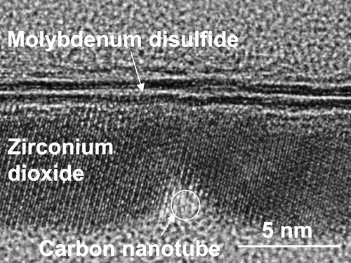
以穿透是顯微鏡拍攝的1奈米電晶體截面,可看到1奈米大小的碳奈米管閘極以及二硫化鉬通道,以二氧化鋯絕緣體隔開
(來源:Sujay Desai/UC Berkeley, Lawrence Berkeley National Laboratory)
以上策略已經奏效,但還需要更進一步最佳化才能使其性能媲美目前的矽電晶體。其他研究團隊成員還包括加州大學柏克萊分校(UC Berkeley)教授Chenming Hu、德州大學達拉斯分校(University of Texas at Dallas)教授Moon Kim,以及史丹佛大學(Stanford University)教授Philip Wong。
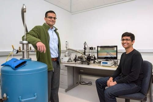
勞倫斯柏克萊國家實驗室的Ali Javey教授(左)與他的研究所學生Sujay Desai
(來源:Marilyn Chung, Lawrence Berkeley National Laboratory)
編譯:Judith Cheng
(參考原文:One-Nanometer Transistor Demonstrated,by R. Colin Johnson)
For more than a decade, engineers have been eyeing the finish line in the race to shrink the size of components in integrated circuits. They knew that the laws of physics had set a 5-nanometer threshold on the size of transistor gates among conventional semiconductors, about one-quarter the size of high-end 20-nanometer-gate transistors now on the market.
Some laws are made to be broken, or at least challenged.
A research team led by faculty scientist Ali Javey at the Department of Energy’s Lawrence Berkeley National Laboratory (Berkeley Lab) has done just that by creating a transistor with a working 1-nanometer gate. For comparison, a strand of human hair is about 50,000 nanometers thick.
“We made the smallest transistor reported to date,” said Javey, lead principal investigator of the Electronic Materials program in Berkeley Lab’s Materials Science Division. “The gate length is considered a defining dimension of the transistor. We demonstrated a 1-nanometer-gate transistor, showing that with the choice of proper materials, there is a lot more room to shrink our electronics.”
The key was to use carbon nanotubes and molybdenum disulfide (MoS2), an engine lubricant commonly sold in auto parts shops. MoS2 is part of a family of materials with immense potential for applications in LEDs, lasers, nanoscale transistors, solar cells, and more.

Berkeley Lab faculty scientist and UC Berkeley professor Ali Javey (left) and graduate student Sujay Desai created the smallest transistor to date. Next to them is a vacuum probe station used to measure the electrical characteristics of the 1-nanometer-long transistors. (Credit: Marilyn Chung/Berkeley Lab)
The findings werepublished today in the journal Science. Other investigators on this paper include Jeff Bokor, a faculty senior scientist at Berkeley Lab and a professor at UC Berkeley; Chenming Hu, a professor at UC Berkeley; Moon Kim, a professor at the University of Texas at Dallas; and H.S. Philip Wong, a professor at Stanford University.
The development could be key to keeping alive Intel co-founder Gordon Moore’s prediction that the density of transistors on integrated circuits would double every two years, enabling the increased performance of our laptops, mobile phones, televisions, and other electronics.
“The semiconductor industry has long assumed that any gate below 5 nanometers wouldn’t work, so anything below that was not even considered,” said study lead author Sujay Desai, a graduate student in Javey’s lab. “This research shows that sub-5-nanometer gates should not be discounted. Industry has been squeezing every last bit of capability out of silicon. By changing the material from silicon to MoS2, we can make a transistor with a gate that is just 1 nanometer in length, and operate it like a switch.”
When ‘electrons are out of control’
Transistors consist of three terminals: a source, a drain, and a gate. Current flows from the source to the drain, and that flow is controlled by the gate, which switches on and off in response to the voltage applied.

Transmission electron microscope image of a cross section of the transistor. It shows the 1-nanometer carbon nanotube gate and the molybdenum disulfide semiconductor separated by zirconium dioxide, an insulator. (Credit: Qingxiao Wang/UT Dallas)
Both silicon and MoS2have a crystalline lattice structure, but electrons flowing through silicon are lighter and encounter less resistance compared with MoS2. That is a boon when the gate is 5 nanometers or longer. But below that length, a quantum mechanical phenomenon called tunneling kicks in, and the gate barrier is no longer able to keep the electrons from barging through from the source to the drain terminals.
“This means we can’t turn off the transistors,” said Desai. “The electrons are out of control.”
Because electrons flowing through MoS2 are heavier, their flow can be controlled with smaller gate lengths. MoS2 can also be scaled down to atomically thin sheets, about 0.65 nanometers thick, with a lower dielectric constant, a measure reflecting the ability of a material to store energy in an electric field. Both of these properties, in addition to the mass of the electron, help improve the control of the flow of current inside the transistor when the gate length is reduced to 1 nanometer.
Once they settled on MoS2 as the semiconductor material, it was time to construct the gate. Making a 1-nanometer structure, it turns out, is no small feat. Conventional lithography techniques don’t work well at that scale, so the researchers turned to carbon nanotubes, hollow cylindrical tubes with diameters as small as 1 nanometer.
They then measured the electrical properties of the devices to show that the MoS2 transistor with the carbon-nanotube gate effectively controlled the flow of electrons.
“This work demonstrated the shortest transistor ever,” said Javey, who is also a UC Berkeley professor of electrical engineering and computer sciences. “However, it’s a proof of concept. We have not yet packed these transistors onto a chip, and we haven’t done this billions of times over. We also have not developed self-aligned fabrication schemes for reducing parasitic resistances in the device. But this work is important to show that we are no longer limited to a 5-nanometer gate for our transistors. Moore’s Law can continue a while longer by proper engineering of the semiconductor material and device architecture.”
The work at Berkeley Lab was primarily funded by the Department of Energy’s Basic Energy Sciences program. Some of this research was conducted at the Molecular Foundry, a DOE Office of Science User Facility.
###
Lawrence Berkeley National Laboratory addresses the world’s most urgent scientific challenges by advancing sustainable energy, protecting human health, creating new materials, and revealing the origin and fate of the universe. Founded in 1931, Berkeley Lab’s scientific expertise has been recognized with 13 Nobel prizes. The University of California manages Berkeley Lab for the U.S. Department of Energy’s Office of Science. For more, visit www.lbl.gov.
DOE’s Office of Science is the single largest supporter of basic research in the physical sciences in the United States, and is working to address some of the most pressing challenges of our time. For more information, please visit science.energy.gov.
Updated: October 7, 2016
Source:http://newscenter.lbl.gov/2016/10/06/smallest-transistor-1-nm-gate/
Source:http://science.sciencemag.org/content/354/6308/99


 留言列表
留言列表