雖然傳統的製程微縮得以在晶片中填入更多的電晶體,卻使得晶片永遠處於更「黑暗」的狀態,而新興的單晶片 3D 技術可望讓晶片得以「重見光明」。
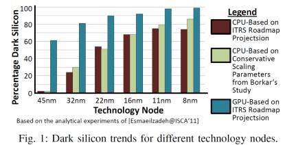
「暗場矽晶」(dark silicon)指的是晶片中必須斷電以避免過熱的部份。在2014年的國際電子元件會議(IEDM)上,ARM的總工程師Greg Yeric指出,在20nm技術節點(包括16/14nm FinFET )時,暗矽的部份預計將佔整個晶片面積的1/3,而到了5nm技術節點時還將增加到佔80%的面積。
如今,製程微縮不再遵循Dennard's Law,在更薄閘電介質時越來越難以避免漏電急劇增加,「因此,儘管幾何尺寸持續微縮,閾值電壓卻未隨之降低。」

不同技術節點的暗矽趨勢
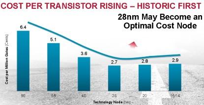
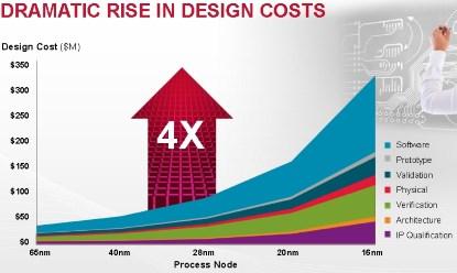
一旦考慮到晶片成本,這種黑暗的前景似乎更是雪上加霜。在最近的SEMI產業技術論(ISS),博通(Broadcom)總裁兼執行長Scott McGregor表示,呈指數上升成本將對產業帶來變化:

每電晶體成本持續攀升

設計成本急劇增加
這為半導體產業描繪了一個非常黑暗的未來。為了開發使用更昂貴電晶體的設計,我們更需要指數級的投資。因此,Scott McGregor總結指出這個「半導體產業前進的重大變化」將是不可避免的。
為了尋找隧道盡頭的一線曙光,ARM技術長Mike Muller提出以下三點建議:
.推動如絕緣矽(SOI)等新的晶片技術進展
.利用高能效、高密度的記憶體來填補部份的「暗場」
.結合最佳製程技術,以 3D IC 實現各種不同的功能。 3D IC 將「成為我們提供高能效解決方案的關鍵部份」。
的確,Sony日前宣佈加入FDSOI Club,未來可望「使其GNSS晶片功耗從10mW降低至1mW。」
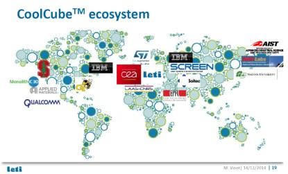
在IEDM 2014,多個研究論文都提出了單晶片 3D 技術與記憶體,如 RRAM 可在邏輯元件頂端成形為後段製程(BEOL)的一部份,有效地形成單晶片 3D 電路。此外,單晶片 3D 的一般情況是,上層電晶體自然形成SOI,因而可透過結合降低閾值的 SOI 達到功效提升,同時降低平均導線長度,並進一步降低導線功率與延遲。CEA Leti攜手ST Micro、IBM與高通(Qualcomm)等公司,發表了單晶片 3D 技術 CoolCube ,可進一步實現 3D VLSI 微縮。下圖顯示CEA Leti發表期望在未來打造的全球單晶片 3D 生態系統。

單晶片3D生態系統
單晶片 3D 技術可望帶來更廣闊的光明前景。直到最近,邁向單晶片 3D 的道路必須變更至前段製程(FEOL)。 FEOL 的製程改變一直是微縮的一部份,但它相當昂貴,而且大多只能由技術先進的主要業者來進行。如今,隨著新興的精確接合機(如EVG或Nikon推出的產品)等工具進展,改變了單晶片 3D 技術的遊戲規則。「...真正的單晶片 3D IC 並不需要新的電晶體資訊配方。現有的任何晶圓廠就能在製程技術上因應變化調整,為一系列的產品功能強化提供非常具有競爭力的成本,以及透過微縮為更好的產品組合提供長期的發展藍圖。」
最終的結果是,雖然傳統的製程微縮看起來將使晶片永遠處於更「黑暗」的狀態,但新興的單晶片 3D 技術可望讓晶片得以「重見光明」。
編譯:Susan Hong
(參考原文: Dark Silicon -- Are the Dark Days Coming?,by Zvi Or-Bach)
Although traditional dimensional scaling looks ever darker, the emerging monolithic 3D technology is poised to bring back the light.
The term "dark silicon" refers to those portions of a device that need to be shut down in order to avoid overheating. In a recent IEDM 2014 short course by ARM's principal engineer, Greg Yeric, dark silicon was projected to account for "about one-third of total area in the 20nm technology node (including 16/14nm FinFETs), increasing to as much as 80% by the 5nm node," as reported by a recent Darker Silicon blog. Unlike the time that dimensional scaling could follow Dennard's Law, it is now getting harder to thin the gate dielectric without causing extreme rise in device leakage, and "as a result, while feature sizes have continued to shrink, threshold voltage has not." The following chart is from a DAC 2013 paper titled The EDA Challenges in the Dark Silicon Era:
This dark outlook seems even darker once the cost of this silicon is taken into account. At the last SEMI Industry Strategy Symposium (ISS), as reported in a blog titled Exponentially Rising Costs Will Bring Changes, Scott McGregor, President and CEO of Broadcom, presented the following charts:
This paints a very dark future for the industry. We would need to invest exponentially more in order to develop designs that use more expensive transistors, of which we would need to keep dark an increasing proportion. It seems that the Broadcom CEO's conclusion -- "major changes for the semiconductor industry moving forward" -- is unavoidable.
Looking for the light at the end of the tunnel, we can turn to ARM's CTO, Mike Muller, in a Cadence blog titled ARM Keynote: Will 'Dark Silicon' Derail The Mobile Internet? When he said "So how to light things up?" Muller started with three suggestions as follows:
- Push forward on new silicon technologies such as silicon-on-insulator (SOI).
- Use energy-efficient, high-density memories to fill some of the "dark" space.
- Combine the best process technologies to fulfill various functions with 3D ICs, which will "become a critical part of how we deliver power-efficient solutions."
Indeed, just this week it was reported in EE Times that Sony Joins FDSOI Club, which included a comment that "Sony was able to cut power consumption in its GNSS chip from 10mW to 1mW."
And at IEDM 2014 we could see multiple papers on monolithic 3D technologies and memories such as RRAM being formed as part of the back-end-of-line (BEOL) on top of the logic, effectively forming monolithic 3D circuits. It should be pointed out that -- in the general case of monolithic 3D -- the upper transistor layers are naturally SOI, so achieving increased power efficiency by combining the SOI reduction of transistor threshold while reducing the average interconnect length further reduces interconnect power and delay. CEA Leti had a workshop presenting their momentum on monolithic 3D through collaboration with ST Micro and IBM, and supported by Qualcomm, titled CoolCube, a powerful approach for further 3D VLSI scaling. The following chart from Leti presentation illustrates the monolithic 3D build up of worldwide ecosystem:
And the monolithic 3D light grows even brighter. Until recently, the path to monolithic 3D required change to the front-end-of-line (FEOL) process. An FEOL process change is always part of dimensional scaling, but it is expensive and -- in most cases -- undertaken only by the leading edge companies. Now, as was presented at the recent IEEE S3S 2014 conference, the emerging precise bonders -- e.g., from EVG or Nikon -- enable a Game Changer for Monolithic 3D; i.e., "…true monolithic 3D IC without the need for a new recipe for transistor formation. The process could be adapted by any current fab providing very competitive costs for a range of product enhancements and offer a long term road map for better offerings by scaling up."
The end result is that, although traditional dimensional scaling looks ever darker, the emerging monolithic 3D technology is poised to bring back the light.
PS A good conference to learn about emerging technologies, such as the IEEE SOI-3D-Subthreshold (IEEE S3S) 2015 conference, which will be held October 5th through 8th, 2015, in Sonoma, California.


 留言列表
留言列表