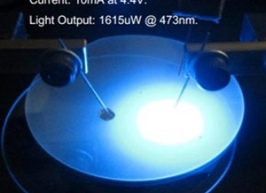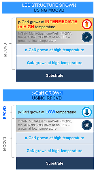

Australian Cleantech company, BluGlass Limited, has demonstrated the best ever p-GaN light output using the company's propriety technology, Remote Plasma Chemical Vapour Deposition (RPCVD) on an MOCVD partial LED structure.
The result is greater than a 10 fold improvement in LED efficiency compared the first p-GaN demonstration data published by the company in December 2012, when the same measuring methodology is applied.
The performance upgrade was achieved by making improvements in addressing the 'interface challenge', a key technical hurdle that has been limiting the p-GaN performance demonstration in the past.
The improvements are the result of the enhanced plasma system in combination with new process steps which are now yielding continuing performance improvements.
BluGlass Chief Technology Officer, Dr. Ian Mann said: “The RPCVD p-GaN based LED performance in the last month has undergone a step change improvement. This has been achieved by focusing on two key aspects – the process steps for initiating the RPCVD p-GaN growth; and in finalising the last layers grown by MOCVD – in effect, making sure the RPCVD and MOCVD steps are compatible. Following these recent developments, we are confident that the team is on the right path to demonstrate that low temperature RPCVD can enhance the performance of LEDs fabricated solely by MOCVD today.”
BluGlass is aiming to demonstrate to the industry that an RPCVD top layer (the p-GaN layers) can improve the light output of an LED.
Additionally, the next generation RPCVD System, the BLG-300, is nearing completion and is expected to be growing GaN later this month. This ex-production scale system is a significantly larger system than the current R&D workhorse and will effectively double BluGlass’ research and development capacity. Having multiple RPCVD systems will greatly enhance the team’s capability to address the LED milestones, the scaling of the technology towards 8-inch wafer deposition and the potential performance advantages of a low temperature CVD process for GaN on silicon.

RPCVD offers LED manufacturers many potential benefits.
The bulk of commercial LEDs are today made using a process commonly called MOCVD (metal organic chemical vapour deposition). MOCVD is a highly complex process that is used to deposit very thin layers of atoms onto a substrate to produce important compound semiconductor materials such as gallium nitride (GaN).
GaN is now an important material used in light-emitting diodes (LEDs), lasers, transistors, electronic and opto-electronic devices.
BluGlass has invented a process using remote plasma chemical vapour deposition (RPCVD), which is also a chemical vapour deposition (CVD) process, but one that offers unique advantages over the MOCVD platforms of today.
In order to explain how RPCVD is a beneficial approach to CVD, it is helpful to understand some of the basics of the incumbent technology.
How MOCVD Works
MOCVD is a method used to deposit (grow) semiconductor films onto a substrate (wafer). When producing gallium nitride (GaN), organometallic compounds are reacted with ammonia inside a deposition chamber. This gas mixture is precisely delivered to a heated substrate (up to approximately 1,200°C).
The precursor molecules undergo pyrolysis (thermal decomposition) leaving the desired atoms, e.g. Ga and N available for growth. These atoms bond at the surface and crystalline layers of GaN are formed in neatly stacked layers.
For the growth of GaN, MOCVD uses toxic ammonia (NH3) as the nitrogen source. MOCVD relies on very high temperatures to effectively break the nitrogen-hydrogen bonds to result in a quality deposition.
How RPCVD Works
RPCVD works in a similar way to MOCVD where chemicals are introduced into the reaction chamber for decomposition.
Whereas MOCVD uses ammonia (NH3) as the source of nitrogen, RPCVD uses nitrogen gas (N2) passed through an electrical coil that generates a plasma. This arrangement provides a direct source of nitrogen used for the deposition of GaN.
The nitrogen plasma generation is not dependent on high temperature to provide a source of reactive nitrogen atoms. This allows for the growth of GaN to be carried out at much lower temperatures than those used in MOCVD while maintaining the critical crystalline quality necessary for high performance devices.
Nitrogen is safer to handle and does not require scrubbing compared to highly toxic ammonia used in MOCVD.
Source:http://www.bluglass.com.au/%EF%BC%83rpcvd-for-led/c1ifp


 留言列表
留言列表