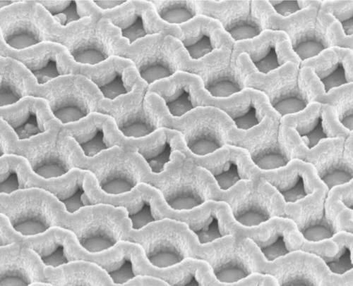
Scanning Electron Micrograph (SEM, scale bar is 200 nanaometers) of tungsten sputtered on the Al2O3 dielectric shells, allowing for a wide variety of materials to be used.
(Image: MIT)
PORTLAND, Ore. — The biggest problem with photovoltaic (PV) panels may have been solved by researchers at the Massachusetts Institute of Technology (MIT). Today, the most efficient solar panels use expensive multi-junctions, each of which capture a different part of the solar spectrum, but not all of it.
MIT's solution is to put an intervening material between the sun and a normal infrared PV panel. This designer material absorbs the entire solar spectrum, reflects light outside the solar spectrum, and glows infrared (heat) with the total power absorbed from the sun. MIT calls it solar thermophtovoltaics (STPVs).
Jeff Chou, a post-doctoral researcher at MIT, working with professors Nick Fang, Evelyn Wang, and Sang-Gook Kim, told EE Times:
To increase the efficiency in solar thermophotovoltaic (STPV) systems they require a material that only absorbs across the solar spectrum and reflects light outside of the solar spectrum. The reason is to minimize thermal radiation losses in the infrared. When this is achieved, the solar energy can be efficiently stored as heat with minimal losses. STPV systems also require a selective emitter that radiates thermal energy to a photovoltaic. In order to maximize efficiency, only radiated energy above the bandgap of the photovoltaic should be emitted, and thus a selective emitter is also required. The material we developed with 2D metallic dielectric photonic crystals is potentially capable of serving as both the selective absorber and selective emitter functions to boost the overall efficiency of STPV systems.
(Image: MIT)A metallic dielectric photonic crystal with solar broadband, omni-directional, and tunable selective absorption with high temperature stable properties is fabricated on a 6" silicon wafer.
The team's material should technically be called a planar photonic crystal, since it is not actually a 2D monolayer, but is studded with rings the width of which determine the spectrum of light they absorb. The researchers, however, insist on calling it a 2D material because planar dimensions, not it thickness, determines its advantageous properties.
"We call it a 2D photonic crystal, because it is periodic in two dimensions (x and y). Thus the name 2D is what is commonly used in the photonics community for such materials," Chou told EE Times. "So the 2D I mention is in regards to the periodicity and is not in reference to an actual atomically flat 2D material."
Regardless of definitions, the planar periodic photonic crystal can be tuned across the entire spectrum of solar energy, and naturally reflects any wavelengths outside that spectrum. To boot the material is able withstand temperatures over 1,000 degree Celsius (1,832 degrees Fahrenheit), making it ideal for solar concentrators, plus is able to absorb nearly equally well at angles up to 70 degrees so that expensive mechanical tracking systems do not have to be included.
"Along with a wide spectral property, an ideal, practical solar absorber should be tuneable, absorb at wide angles, be stable at high temperatures, and be mass manufacturable for low cost reasons. The absorber we developed is the only one that has all of these properties, making it an ideal absorber," Chou told EE Times.
Previous versions of the prototype in an earlier project did not fill the cavities with dielectric, but were left open to the air. This still allowed the material to be tuned to the sun's frequency spectrum, but not trap the thermal energy there which led to inefficiencies. Earlier versions also required small metallic substrates, but the current fabrication method can be run on any standard CMOS line of any size -- even 12-inch wafers.
The researchers plan to experiment with using different metals than the relatively expensive ruthenium used today, which they believe is feasible since the chemical properties of ruthenium do not come into play with the process. Chou is also working with Kim on applications and expects commercialization of the technique to take five years.
Also contributing to the project was MIT research scientist Ivan Celanovic and former graduate students Yi Yeng, Yoonkyung Lee, Andrej Lenert, and Veronika Rinnerbauer. Funding was provided by the Solid-State Solar Thermal Energy Conversion Center and the US Department of Energy.
Get all the details at Enabling Ideal Selective Solar Absorption with 2D Metallic Dielectric Photonic Crystals.
— R. Colin Johnson, Advanced Technology Editor, EE Times
Source:EETimes


 留言列表
留言列表