SAN JOSE, Calif. — A microprocessor research project cancelled by Oracle gives a glimpse into the future of high-end chip design at a time when traditional scaling is slowing down. The proposed Sparc CPU aimed to use chip-stacking techniques still in development to get advantages increasingly hard to squeeze out of silicon process technologies.
The researcher behind the concept was part of a layoff in Oracle’s hardware group earlier this year. But his ideas live on at a new consulting firm already working with one Silicon Valley semiconductor company.
“The more I look into this, the more I am convinced it is the way to go,” said Don Draper, former senior principal engineer at Oracle who now heads ProPrincipia, a three-person company that he formed.
“Computational density is not growing as fast as internet traffic, and the amount of data for analysis in the data center is growing even faster. To solve this problem, you need more memory bandwidth, and that’s one area where 3D stacking shows its promise.”
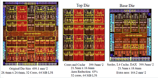
In a conference late last year, Draper showed how existing Sparc processors could be redesigned into two smaller, stacked die. One packs just the cores and caches, and another, made in an N-1 or -2 node running at half the data rate, carries peripherals such as serdes, an L4 cache, and on-chip network — reducing costs and power.
Alternatively, the new chips could nearly double the number of cores and L3 cache, especially if the stack adopts emerging microfluidic-cooling techniques. “You can get twice the performance in the same technology node,” said Draper.
Emerging die-stacking techniques are ideal for bonding a host processor with an accelerator for memory-intensive jobs such as machine learning, said Draper. By contrast, chip-to-chip interconnects such as CCIX and OpenCAPI, “are like sucking on a soda straw.”
Draper also suggested use of integrated voltage regulators (IVRs) in the trailing-edge die. Using relatively small magnetic inductors, he estimated that IVRs can save power and area on the board and boost the chip’s data rate by as much as 150 MHz.
Nevertheless, he admitted that “[his] proposal for Oracle to implement [chip stacks] in a top-of-the line M-class processor would have required … a huge risk and a gigantic commitment.” For example, “if there was any problem implementing [the stack], the top die would be unusable.”
The chip stacks use through silicon vias (TSVs), which have been used in memory stacks in which structures are regular but are tricky for dense, irregular logic chips. The TSVs can be relatively thick with keep-out zones around them.
Draper claims that problems dissipating heat through the stack have largely been resolved. Copper interfaces with high thermal conductivity can readily dissipate heat from a relatively cool bottom die through the heat sink or fan in the hotter top die.

The Invensas division of Xperi Corp. is one company pioneering the kind of room-temperature wafer- and die-bonding techniques that Draper thinks microprocessor designers will use. DRAM stacks are its next big target with hopes for products in 2019, followed by a wide variety of processors, ASICs, GPUs, and FPGAs.
“Our intent is to talk to customers now; we want to get their wafers because everyone has a slightly different process and TSVs,” said Invensas president, Craig Mitchell. Another hurdle is avoiding contamination from tiny particulates created when wafers are diced.
“We’re making good progress, showing four-high DRAM stacks. We’re starting with 3D DRAM because it’s a high-volume market, and if you can demonstrate in DRAM, it tends to be easier to move the technology elsewhere.”
Invensas got its foothold stacking CMOS imagers using a wafer-to-wafer technique bonding oxides at pitches of 6 to 14 microns for Sony and others.
Sometime next year, Invensas hopes to take the next step, applying the process to seal groups of MEMS sensors.
Next, it aims to apply its emerging die-level Direct Bond Interconnect to connect MEMS sensors to logic chips. It already licensed its technology to Teledyne Dalsa, which runs a large MEMS foundry.

Ultimately, Invensas aims to make DBI interconnects that are smaller than a single micron to enable turning big chips into arrays of stacked chiplets. Others are attacking this space, too, seeking lower-cost alternatives to 2.5D stacks that lay die side by side on relatively large, expensive silicon interposers.
In March, TSMC announced that it is developing a version of its wafer-level fan-out package for high-performance computing called InFO, currently used for mobile applications processors. It also is expanding its 2.5D CoWoS process to handle as many as eight HBM2 DRAMs on substrates up to 1,500 mm2.
The 40-micron I/O pads and 65-mm2 substrates of the expanded InFO won’t compete with the larger, denser chips that Invensas targets with DBI, said Mitchell. However, Mediatek recently announced that it would use InFO for a data center chip, suggesting that the technology is expanding its reach, said Emilie Jolivet, a packaging analyst at Yole Développement.
DBI and InFO are like apples and oranges, said Mitchell. InFo is a packaging technology translating fine-pitch chip connections to coarse pitch-printed circuit board links; DBI is a chip-to chip interconnect using fine-pitch connections.
For example, the Apple’s A10 apps processor uses InFO to translate 220-micron pitches in a die interface to a 350-micron interface for a printed circuit board. By contrast, DBI is being tested using 40-micron contacts between DRAMs that could someday be stacked eight high, he said.
For its part, Intel aims to address the trend with its Embedded Multi-Die Interconnect Bridge. The EMIB technology initially used to link external serdes to a large FPGA “could change the game and enlarge the packaging horizon,” said Jolivet.
Mitchell said that EMIB is not a direct competitor to DBI and questioned how far it can scale. DBI’s biggest rival, today’s thermal compression techniques, are currently limited to 25-micron or larger interconnects. “That 25-micron pitch seems to be a tough wall to break through,” he said.
Yole said that Apple’s use in its A10 apps processor of TSMC’s InFO “was a turning point for fan-out packaging” last year. In a recent report, it predicted that both equipment and materials markets for such techniques will see 40% compound growth.
— Rick Merritt, Silicon Valley Bureau Chief
Source:EE Times


 留言列表
留言列表