Along these years, the company has refined and patented its technology, creating a full 3-axis MEMS-based AFM probe on a 1x1mm silicon chip. The electrothermal actuation they developed (using arrays of thermal bimorph actuators) for both the lateral and the vertical movements of the probe tip does not suffer from creep or hysteresis while achieving high natural frequencies in the kHz range, enabling long-term imaging experiments. It also allows interesting scanning modes, such as simultaneous topographical and thermal metrology, as ICSPI unveiled at the 29thIEEE International Conference on Micro Electro Mechanical Systems last year.
"It is only over the last couple of years that we were able to make our MEMS AFM probes robust and reliable enough for commercialization", told us Neal Sarkar, Co-Founder of the company during a phone interview.

scanning probe and a sample to be imaged.
Only a few weeks ago, ICSPI made its first commercial launch with a complete atomic force microscope based on its MEMS AFM tip, the nGauge. The whole unit measures only 70x90x75mm, weighs 450 grams and comes with several scanning range options up 20x20x10μm (xyz). It costs less than $10,000 or a fraction of the price of your typical booth-sized AFM while being fully automated (to approach the sample) and the staff at ICSPI claims the instrument is so simple to operate that a 10-year old can start imaging samples with nanoscale precision in under a minute.
With this launch, ICSPI hopes to democratize AFMs, making the instrument as commonplace as the optical microscopes you would find in any lab. Starting with small series, for now, the instruments are assembled manually at the company's premises. But even though the privately-owned 5-staff company may be very close to reach the breakeven point, covering its operational expenditures through the sale of a few hundred units, the story doesn't end up here. "Strategically, we had to think carefully. We are not trying to make money on the AFM stage, in fact we share all the mechanical drawings and we use open source software so anyone could buy our AFM tips and design their atomic force microscope. The value is in the chip", noted Sarkar.


Indeed, although the MEMS AFM scanning tip lasts about ten times longer than today's $25+ AFM tips, it can be considered as a consumable. For approximately $250, users can replace the tiny AFM probe (in case it breaks or wears out), and what they get is not only a brand new tip, but also the scanners and sensors integrated with it, so the instrument stays fresh and up to date with ICSPI's latest improvements in tip shape, scan range, scanner linearity, and sensor performance.
The company currently manufactures at the die-scale, which isn't nearly as economical as wafer-scale. Once it makes the jump to wafers, it hope to be able to reduce the cost of these consumables.
But how do you sell even more tips than you possibly could with standalone AFMs units?
The bulk of the business for the company, where premiums may be paid, certainly lies in the integration of their technology into large area in-situ metrology solutions.
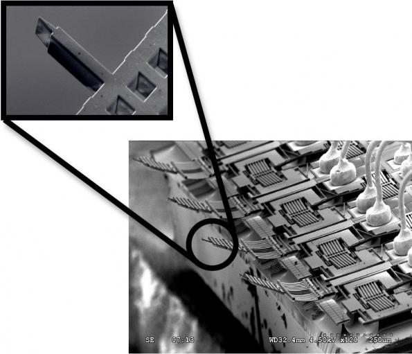
In a paper titled "A Single-Chip Scanning Probe Microscope Array" the team presented last January at MEMS 2017, ICSPI somehow unveiled its roadmap. The paper detailed the design and fabrication of a 4x1 array of AFM cantilevers sharing the same electrothermal lateral stage but independently driven, sensed, and controlled. Designed for high throughput metrology, the quad-AFM tip was not just a proof of concept.
"We've decided to architecture our AFM probes in a modular way, so we can build arrays easily" admitted Duncan Strathearn, Director of Product Development at ICSPI. "In the near term, we'll launch other modes of scanning, contact-, thermal-, microwave-modes before we work on large arrays."
Because the MEMS designs and the technology require a lot of know-how, ICSPI is keen about partnering with key wafer inspection and metrology tool vendors for which it could design bespoke multi-tip MEMS AFM probes.
"We'd love to partner with the likes of KLA Tencor or Cascade Microtech to develop wafer-level tools. We've talked to a couple of probe system manufacturers who are prototyping our AFM tips at the end of an XYZ manipulator, but developing the tools require some collaboration" Strathearn said.
"The standalone units are getting traction from academia but the industry has been suddenly interested by its low cost and simplicity of use for metrology applications in roll-to-roll manufacturing. For example they need to measure the average roughness of their films, the granularity of deposited particles, or the homogeneity of sputtered OLED material".
In the semiconductor industry, there are automated defect inspection tools that rely on electron beams and machine vision, they can perform multi-point inspections but they are usually slow and costly.
Strathearn envisages 1000-point inspection systems capable of simultaneous inspection across all probing points. "A custom probe-card is simple enough to design. We can have 30,000 MEMS AFM dies on a single wafer", he said, hinting that since all the driving electronics could be integrated or stacked, a full wafer-level probe with 1000 active inspection points would have 30 probes' life worth.
"We use Al2O3 at the tip of our AFM probe, which is almost as hard as sapphire, and we've demonstrated over 1000 scans without measurable wear" he added, highlighting that ICSPI's solution is not only smaller and cheaper but also more robust.
The company is busy investigating new methods to further improve the aspect ratio of their wedge-shaped scanning tip. It is also looking at developing through silicon via interconnects for its MEMS that would eliminate wire-bonding and allow for dense arrays.
Visit ICSPI (Integrated Circuit Scanning Probe Instruments) at www.icspicorp.com
Related articles:


 留言列表
留言列表