
根據市場研究公司Yole Developpement的調查報告,次世代顯示技術——microLED市場可望從2018年開始快速成長,但在此之前必須先克服一些既有的挑戰,以及建立其供應鏈。
相較於有機發光二極體(OLED),微發光二極體(microLED)以傳統的氮化鎵(GaN) LED技術為基礎,但採用單片方式製造顯示器,總亮度可達到OLED產品的30倍,如果以每瓦流明(lux/W)的方式來看,它提供了更高的效率。
根據Yole,microLED最初將成功應用於智慧手錶,並加速該技術與供應鏈的成熟,從而讓microLED接著在高階電視、平板電腦與筆記型等應用領域發展成為OLED的競爭技術。雖然microLED並不至於為這些應用帶來重大顛覆力量,但仍兼具了OLED與LCD的最佳優勢。Yole的姐妹公司KnowMade也指出,在2000至2016年間在microLED領域就有超過1,570項專利的申請和授權。
Yole的預測,microLED顯示器市場將在2019年開始成長,並在2025年到3.3億台的出貨量。而智慧型手機導入microLED顯示器的應用預計要到2021年以後,但預計隨後將快速進展到超過50%的顯示器市場佔有率。
microLED顯示器市場將在2025年到3.3億台的出貨量(來源:Yole Developpement)
microLED是一種發射顯示技術,提供了較高的對比度與速度,以及廣視角。相較於OLED顯示器,microLED還提供了更廣色域、更高數十倍的亮度、更低功耗以及更長的壽命。此外,microLED易於整合感測器與電路,可輕鬆打造具有指紋辨識和手勢控制等嵌入感測能力的薄型顯示器。

microLED顯示器尚待克服的既有挑戰(來源:Yole Developpement)
Sony在2016年製造了一款LED視訊顯示器,以microLED取代傳統封裝的LED。然而,較大規模的消費應用將出現在智慧手錶——這是由蘋果(Apple)在2014年收購新創公司Luxvue後所帶動的新消費領域。microLED由於具有提供高亮度與低功耗的特性,預計最終也將在擴增實境與混合實境(AR/MR)顯示器佔主導地位。

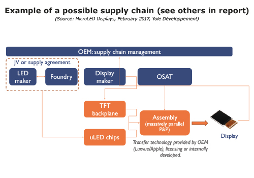
microLED顯示器供應鏈示例(來源:Yole Developpement)
編譯:Susan Hong
(參考原文:MicroLED display market poised for lift off,by Peter Clarke)
With the increasing success of organic light emitting diodes (OLEDs), and mounting interest in quantum dot (QLEDs), emissive technologies have already proven their worth and enabled a variety of consumer products with stunning display performance. But now, microLEDs could be another disruptive display technology for a variety of applications.
Since Apple acquired start-up Luxvue in 2014 and Facebook-Oculus acquired InfiniLED last year, this new format of inorganic LEDs has generated a lot of attention. Yole Développement (Yole) explores why in its new report on MicroLED Displays. Eric Virey, Yole Senior Analyst and the report’s author has been telling us what we can expect from this technology – read on to find out more.
Yole Développement (YD): Could you explain what microLED displays are and what differentiates them from other established technologies such as LCD or OLED?
Eric Virey (EV): MicroLED displays are similar to OLEDs in the sense that they are an emissive technology. Each pixel is a tiny light emitter whose brightness can be individually controlled. This is unlike LCD technologies, in which the light is generated by an LED backlight and goes through a matrix of “light switches”, which are the liquid crystals. Each of those switches can be individually controlled to block or transmit the light through color filters that constitute the individual red, green and blue subpixels. LCD overall optical efficiency is typically very low, around 5-10%. Most of the light is wasted.

YD: What are the other advantages of microLEDs?
EV: They retain all the benefits of OLEDs in term of contrast, color rendering, fast refresh rates and wide viewing angles. But because the light emitting materials are inorganic, they have much better environmental stability, lower power consumption and can deliver exceptionally high brightness. We’re talking orders of magnitude higher than established technologies. In addition, because each individual emitter can be made in very small dimensions compared to the pixel pitch, they enable the integration of additional components such as infra-red emitting LEDs and sensors within the display front plan. These could potentially be used to deliver various functions such as motion sensing, fingerprint readers or local brightness adjustment.
YD: What are the challenges associated with this technology?
EV: OLEDs can be grown directly on the thin film transistor matrix that controls each emitter. Unfortunately, this isn’t possible with inorganic LEDs. The process temperature and harsh atmosphere would destroy the transistor matrix and there is no technology to make LEDs over very large surfaces. MicroLED display assembly is therefore inherently complex. Each subpixel emitter has to be manipulated individually and connected to the driving transistors. A 4K displays has close to 25 million such sub-pixels. Using traditional pick and place equipment, it would take more than a month to assemble a single TV! The industry therefore had to develop technologies to manipulate tens of thousands to millions of microLEDs simultaneously.
The problems are compounded by the very small size of the emitters. For most applications, lateral dimensions below 10 µm would be necessary to keep LED epiwafer cost low and make the display economical. Manipulating such small objects on a massive scale is a paradigm shift for the industry. The small dimensions also create additional challenges in terms of LED epitaxy and manufacturing. Micron scale defects can be tolerated on traditional LEDs that are 100s of microns in length, but become killer defects with microLEDs. This means that cleaner manufacturing environments are required. Maintaining high LED efficiency at such small dimensions is also a challenge. In the MicroLED Displays report, we describe in detail the challenges that need to be tackled and how to overcome them.
YD: What are the applications for microLED displays?
EV: Conceptually, any type of display can be built with MicroLEDs. Sony demonstrated a full HD microLED TV in 2012 and introduced the first commercial large video display in 2017, although we don’t strictly consider the latter a microLED application. The emitter size fits the definition but I’d describe it more as a “Chip On Board” technology.
The economics of microLEDs are different from LCD and OLED. The backplane is similar to what is used for OLEDs, but the frontplane cost scales with the number of pixels rather than with the surface area. This potentially makes applications such as TVs quite attractive. However, the transfer costs tend to scale with the pixel pitch. So ultimately, the most suitable applications for microLEDs are those with a low number of pixels and high pixel density. This makes wearables such as smartwatches an ideal target. In terms of manufacturability, this is the lowest hanging fruit and in terms of performance, microLEDs would constitute a breakthrough in power consumption and brightness. This was probably the first application Apple had in mind when it acquired Luxvue in 2014 and we believe that if microLEDs ever make it the market in a consumer product, smartwatches are likely to be the first candidate.
Augmented and mixed reality (AR/MR) is another potential killer app. As of today, microLEDs are by far the best positioned technology to deliver the brightness required for the overlaid image that competes with ambient light. MicroLEDs can also deliver the fast refresh rates and high pixel density required for this application. A lot of microLED companies are focusing mostly on AR/MR. Facebook/Oculus has shown its interest by acquiring InfiniLED, a microLED startup, in 2016 and negotiating licenses from other companies.
Ultimately, most display applications could be addressed. Smartphone could be the most challenging. Incumbent solutions such as OLED already deliver excellent performance at a very low cost point. It will be hard but not impossible for microLEDs to compete. Here again, low power consumption could be the differentiator and reducing the emitter size is the key goal to become cost competitive.
YD: Who are the leaders in microLED development?
EV: We did a thorough patent search and analysis with our colleagues at KnowMade and were surprised to see the extent of companies involved in the field. We found many leading display makers, LED makers, many start-ups and a flurry of electronic OEMs and semiconductor manufacturers including Intel! As of today, Luxvue has one of the most comprehensive portfolios. They’re benefiting from Apple’s R&D and execution horsepower and leverage on the supply chain since the acquisition. But many smaller companies have also developed very smart technology bricks. They include Lumiode, VueReal, Mikro-Mesa, Playnitride, and mLED. One also must not forget Sony which has been pioneering the field since its first TV demo in 2012.
YD: What are the remaining obstacles to commercialization?
EV: The science is in place but there are still a variety of technology challenges that need to be resolved, including epitaxy homogeneity and reproducibility among others. MicroLEDs also still suffer from low efficiency compared to what traditional LEDs deliver. This is due to sidewall defects that are detrimental for the smallest dimensions. Efficiently manipulating very small devices, below 10 µm in size, is still a challenge. Progress is being made on all these fronts. However, there are also some supply chain challenges. A lot of the transfer, testing and repair equipment is not available off-the-shelf and will have to be custom-designed. In addition, enabling large scale microLED display manufacturing requires bringing together disparate technologies and supply chain elements, namely LED, thin-film transistor (TFT) backplane and chip transfer. The supply chain is complex and lengthy compared with that of traditional displays. Each process is critical and managing every aspect effectively will be challenging. No single player can solve all the issues and it seems unlikely that any will fully vertically integrate. In the short term, only a highly motivated OEM could have the leverage and financial means to bring those elements together and enable high-volume consumer applications. AR/MR is different. It’s not unrealistic to imagine a well-funded start-up bringing a product to market on its own if it has the support and commitment of larger consumer electronic companies.
Source : ![]()
MICROLED DISPLAYS COULD DISRUPT LCD AND OLED
Micro-light emitting diodes (MicroLED) are an emissive display technology. Just like organic light emitting diodes (OLED), they offer high contrast, high speed, and wide viewing angle. However, they could also deliver wider color gamut, dramatic – orders of magnitude – higher brightness, significantly reduced power consumption and improved lifetime, ruggedness and environmental stability. In addition, microLEDs allow the integration of sensors and circuits, enabling thin displays with embedded sensing capabilities such as fingerprint identification and gesture control.
The first MicroLED commercial product was unveiled by Sony in 2016 in the form of a small-pitch LED video display where traditional packaged LEDs are replaced by microLEDs. The first consumer killer-app could come in the form of smartwatches, propelled by Apple, which invested in the technology by buying Luxvue in 2014. MicroLEDs could also eventually dominate augmented and mixed reality displays thanks to their unique ability to deliver both the brightness and low power consumption required for the application.
Initial success in smartwatches could accelerate technology and supply chain maturation, making microLED competitive against OLED in high end TVs, tablets and laptops. Although less disruptive for those applications, microLED would still bring the best of OLED and liquid crystal displays (LCD) together. Smartphones will be a tough nut to crack and require further technology improvement in the manufacturing and handling of very small microLEDs (< 5 µm). In our most optimistic scenario, the market for microLED displays could reach up to 330 million units by 2025.

THERE ARE MANY ENGINEERING AND MANUFACTURING ROADBLOCKS BEFORE MICROLED REACHES PRIME TIME
The science is here, but microLED is an inherently complex display technology with cost drivers different from those of incumbent technologies. The concept is simple: each pixel is constituted of individual microLED emitters. However, at very small dimensions, microLED operation tends to be dominated by nefarious sidewall effects which impact performance. The reported efficiency of microLEDs below 10 µm side length is often 10-20% of larger LED chips or below. At those levels, microLED displays can’t deliver on the key promise of low energy consumption. Solving this issue is a key priority for companies involved microLEDs. Some such as VueReal or Mikro-Mesa have reported significant improvement.
Efficiently manipulating high volumes of microLEDs and positioning them on the backplane is another major area. Assembling a single 4K display would take more than a month using traditional pick and place equipment! Companies such as Apple, X-Celeprint, Playnitride and others have developed massively parallel pick and place technologies that can process tens of thousands to millions of microLEDs simultaneously. However, the handling of the smaller size (up to 10 µm) chips and positioning accuracy needs further work. Alternatively, companies such as VueReal or Rohinni are developing “semi-continuous” processes akin to traditional printing.
In modern displays, dead or defective pixels are not acceptable. Achieving 100% combined yields in epitaxy, chip manufacturing and transfer is nothing short of utopia. MicroLED display manufacturers must therefore develop effective defect management strategies combining pixel redundancies and/or individual pixel repair depending on the characteristics of the display.
Other challenging technology nodes include color conversion, light extraction and beam shaping, all subjects of intense research, licensing and mergers and acquisition activities.
IF SUCCESSFUL, MICROLED DISPLAYS COULD HAVE PROFOUND IMPACT ON BOTH THE LED AND DISPLAY SUPPLY CHAINS
Many startups and large companies are working on microLEDs, from LED makers such as Epistar, Nichia or Osram to display makers like AUO, BOE or CSOT and original equipment manufacturers (OEMs) such as Apple or Facebook/Oculus.
Enabling large scale microLED displays requires bringing together three major disparate technologies and supply chain elements: LED, thin-film transistor (TFT) backplane and chip transfer. The supply chain is complex and lengthy compared with that of traditional displays. Each process is critical and managing every aspect effectively will be challenging. No single player can solve all the issues and it seems unlikely that any will fully vertically integrate. Small companies could bring together the different technologies to serve the augmented reality (AR) market, but for high volume consumer applications such as mobiles or TVs, only a strong push from a leading OEM can enable a supply chain. Apple is the most likely candidate with enough leverage and financial strength to bring all partners together. Other candidates include Oculus, which has also invested in microLEDs for AR/mixed reality (MR) applications.
Each participant will attempt to capture as much added value as it can. For LED makers, low defect requirements and high resolution features of microLED means large investments in new clean room and lithography equipment which might be better suited to CMOS foundries. Traditional display makers are used to manufacturing both back and front planes in an integrated fashion and delivering finished panels to OEMs. With microLEDs, they will struggle against becoming component suppliers, only providing a TFT backplane to whichever participant will produce the final display assembly: OEMs or outsourced semiconductor assembly and test (OSAT) players.
Some companies will benefit from microLED displays independently of how the supply chain is shaped. These beneficiaries include metal-organic chemical vapor deposition (MOCVD) reactor and other LED equipment manufacturers as well as wafer suppliers. For the latter, however, sapphire manufacturers will have to keep an eye on a possible come back of the old LED-on-silicon idea which could have definite advantages in microLED manufacturing.

Source : ![]()


 留言列表
留言列表