
BESIDES TECHNICAL CHALLENGES, AN IC-LIKE SUPPLY CHAIN IS BEING CONSOLIDATED
YoleDéveloppement在其發佈的「矽光子技術的資料中心與其他應用」(Silicon Photonics for datacenters and other applications)研究報告中分享最新發現。包括Yole資深技術與市場分析師Eric Mounier、ARCH Venture Partners的投資合夥人Jean-Louis Malinge (Kotura前執行長)等專家,均在文中針對矽光子產業進行深入的分析。
目前,矽光子市場還不算太大,估計2015年的銷售額不到4千萬美元,實際上也只有幾家公司開始在開放市場上出貨產品,其中包括Mellanox、思科(Cisco)、Luxtera、英特爾(Intel)、意法半導體(STMicroelectronics)、Acacia與Molex等,都是這一市場的主導業者。
然而,矽光子技術已經持續多年的發展了。如今,這項技術備受Facebook 與微軟(Microsoft)等大型網路公司看好,並且開始積極推動。
「矽光子技術已經達到大規模成長之前的引爆點了,」Eric Mounier指出,「事實上,我們估計以矽光子技術封裝的收發器市場將在未來十年快速成長達到60億美元的市值。」
矽光子是一種令人振奮的技術,它融合了光學、CMOS技術以及先進的封裝技術。這種組合得力於半導體晶圓製造的可擴展性,因而能夠降低成本。根據Yole,在2020年以前,矽光子晶片將遠遠超越 銅佈線的能力,而其解決方案可望部署於高速的訊號傳輸系統中。在2025年及其後,這項技術將更廣泛地用於處理互連多核心與處理器晶片等應用中。Yole分析師認為,以晶片級而言,這一市場預計將在2025年時達到15億美元。
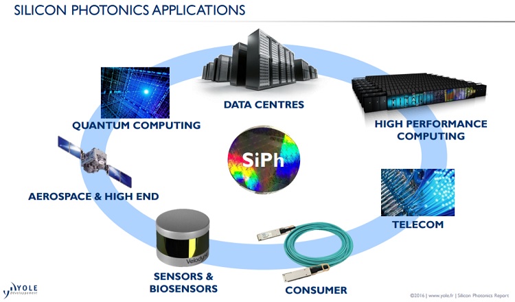
如今,對於矽光子技術而言,資料中心顯然是其最佳機會。當然還有其他許多矽光子學可以利用的新應用,包括高性能的電腦、電信、感測器、生命科學以及量子運算等高階應用。此外,還有兩項新興應用對於矽光子而言也特別令人感興趣——瞄準自動駕駛車應用的光達(Lidar),以及生物化學與化學感測器,均可從整合的光學功能以及進一步的微型化中受益。
光達目前仍是十分昂貴且笨重的儀器,使其在整合至車輛時面臨挑戰。但Yole預期,在2017年時, 具發展前景的先進駕駛輔助系統(ADAS)市場將達到39億美元,其中,基於矽光子技術的光達將扮演關鍵角色。今年八月,美國麻省理工學院(MIT)的光子微系統研究組(Photonic Microsystems Group)發佈成功完成了一項DARPA計劃——採用矽光子實現具有可控發射與接收相位陣列與晶片上鍺(Ge)光探測器的光達單晶片(lidar-on-a-chip)。
生物化學和氣體感測器並不是什麼新技術,其他幾項應用也已經存在一段時間了。隨著具發展前景的大量新興可攜式應用崛起,業界對於氣體偵測的興趣日益重要。將生物化學或氣體感測器整合於智慧型手機或可穿式裝置中,正成為許多公司發展藍圖的一部份,但這一類裝置的尺寸、成本與靈敏度目前仍然存在問題。為了讓光學式氣體感測器更進一步微縮,有些公司已經開始思考採用矽光子技術作為其裝置的整合平台。
不是新的,有一些應用已經存在了一段時間。由於出現了有希望的新的大容量便攜式應用,天氣感測的興趣日益重要。將生物化學或氣體傳感器集成到智能手機或可穿戴設備中目前在許多公司的路線圖上,但是尺寸,成本和靈敏度仍然是問題。為了進一步推動光學氣體傳感器小型化,有些公司考慮以矽光子學作為其設備的集成平台。
此外,根據Yole的矽光子研究報告,在2025年以前,這些非資料中心的應用將達到約3億美元的市場規模。
Have we reached the tipping point before silicon photonics grows massively in data centers?
EXPONENTIAL DATA GROWTH IN DATA CENTERS WILL PROPEL SILICON PHOTONICS TO TAKE OFF INTO OTHER APPLICATIONS, LIKE LIDAR
Big data is getting bigger by the second. Transporting this level of data around with existing technologies will soon reach power consumption, density and weight limits. Photons will continue to replace electrons throughout networks, including in the data center, in the rack and very soon on the board.
Silicon photonics is an exciting technology mixing optics, CMOS technology and advanced packaging. It combines silicon technology’s low cost, higher integration and interconnect density and higher number of embedded functionalities with lower power consumption and better reliability compared to legacy optics.
Massive R&D investments have been made in silicon photonics, but today there are still few products on the market. However, this technology has been strongly pushed by large Webcom companies such as Microsoft, Amazon and Facebook, with investments that will overtake the traditional service providers’ investments in a few years. These Webcom players are targeting $1/Gb prices and are principals for the development of cost-effective photonics technology for future generations of data centers.
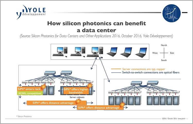
Although copper is still used for top-of-rack switches to servers because the connection distance is short, optical links are becoming mandatory as both bandwidth and communication distance increase. And bandwidth is dramatically increasing close to the rack. Consequently most of the current bandwidth is inside the data center, for distances running from a few meters to a few hundreds of kilometers (see figure 1).
Back in 2000, Bookham was first to commercialize silicon photonics components, namely arrayed waveguide gratings and transceivers. Then in 2006, variable optical attenuators were commercialized by Kotura. These companies have been followed by the likes of Acacia and Intel, who commercialized products in 2016, and ever more products are being launched onto the market, mostly for 100G networks, but soon for 400G (figure 2). The next products will be silicon-photonics based transceivers. But we believe silicon photonics will be then used in other products such as optical bio-sensors, gas sensors and lidars for autonomous vehicles.
Moreover, we see new startups coming and this is a very encouraging sign of growing investments from the venture capitalist community. Fifteen years since the ‘dot com bubble’, it seems the optical communication field is attracting investors again.

A MULTIBILLION DOLLAR MARKET FOR SILICON PHOTONICS IN DATA CENTERS BY 2025, WITH OTHER PROMISING APPLICATIONS AS WELL
The silicon photonics market is still modest with estimated sales below $40M in 2015 and very few companies actually shipping products in the open market. However, we foresee dramatic growth and estimate that the packaged silicon photonics transceiver market will be worth $6B in 10 years.
But besides data centers, which are the best opportunity for silicon photonics technology today, there are many other applications that silicon photonics can enable. These include high performance computers, telecommunications, sensors, life science, quantum computers and other high-end applications.
Two applications are particularly interesting as silicon photonics can push the integration of optical functions and miniaturization further to achieve successful products. Those applications are lidars for autonomous cars and biochemical and chemical sensors.
Lidars are costly and bulky instruments which make their integration in a car challenging. Silicon photonics could allow lidar without moving elements, which can experience issues in a harsh car environment.

Biochemical and gas sensors are not new, and several applications have existed for a while. But we believe that the interest in gas sensing is gaining importance due to the emergence of promising new large volume portable applications. Integration of biochemical or gas sensors into smartphones or wearables is currently on the roadmap of many companies but size, cost and sensitivity are still issues. To push optical gas sensor miniaturization further, some companies are already considering Silicon Photonics as an integration platform for their devices.
These non-data center applications will be about $300M in 2025.
The path to success is not easy, with challenges still to overcome, especially technical ones.
Laser source integration is a major challenge, for which post-processing of laser dies on InP chiplets is an interesting approach.
Power consumption is also important. Today we are at 10pJ/bit and the target is to lower this below 200fJ/bit by 2025.
The industry also needs to move from parallel fibers to wavelength division multiplexing (WDM). Most players have WDM on their roadmap.
Packaging is still a major technical hurdle, accounting for 80%-90% of final transceiver cost. It is a costly process as optical alignment is tight and it increases assembly time. Here, MEMS can be an enabling technology, as exploited by Kaiam and Luxtera, and many initiatives are set up to deliver low-cost photonic assembly pilot lines, especially in Europe.
These technical challenges link to cost, for which the target objective of $5/Gb today must lower to less than $0.1/Gb after 2020.
The silicon photonics supply chain is still under construction (figure 4), lagging years behind the mainstream silicon semiconductor supply chain, with few packaging service or software providers. However, across the world, large R&D acquisitions and programs are being performed, creating intellectual property (IP) positions for the current players. Opportunities will also certainly arise for outsourced semiconductor assembly and test companies because of the need for low cost packaging solutions. Silicon photonics foundries must emerge. It will happen with increasing wafer volumes driving down costs.

Source:YOLE
編譯:Susan Hong
(參考原文:Silicon photonics to become a multibillion dollar market, says Yole ,by Julien Happich)


 留言列表
留言列表