The end of lithographic scaling of DRAM and NAND somewhere between 16nm and sub-10nm has been a popular call for the last few years, with many touting the emergence of new memory types including phase change RAM (PCRAM), ferro-electric RAM (FRAM), magneto-resistive RAM (MRAM), and more recently, resistance RAM as replacements (ReRAM and CBRAM).
Over the years TechInsights has analyzed PCRAM from Numonyx and Samsung, FRAM from Ramtron and MRAM from Freescale and its spin-off Everspin. These devices have found niche applications, but are not seen as replacements for NAND or DRAM due to scaling or power consumption constraints. Resistive RAM, on the other hand, features low power consumption and a small cell area; both compelling reasons for their adoption as a non-volatile memory.
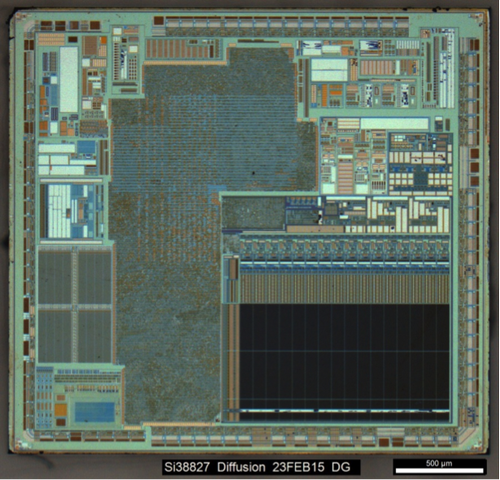
Adesto and Panasonic are two companies that have brought two variations of resistance RAM to market. Adesto offers stand-alone memory chips ranging from 32 kb to 128 kb of conductive bridge RAM (CBRAM) for use in low power applications such as the internet of things (IoT). Panasonic is offering an 8-bit MCU with embedded ReRAM that may be used for portable health care applications, security equipment and sensor equipment. These are still niche applications, so pose little threat to DRAM or NAND in the near future.
Click here for larger image
Click here for larger image
The end of scaling for planer NAND and DRAM is real and the likes of Samsung, Micron, SK-Hynix and Toshiba are working on 3D architectures for these devices. Samsung for example released its 3D V-NAND memory in the fall of 2014 where it is being used in solid state drives (SSD) and AMD is expected to use SK-Hynix’s high bandwidth memory (HBM) in its upcoming 390X GPU.
At TechInsights, we thought it timely to look at products from bothAdesto and Panasonic.
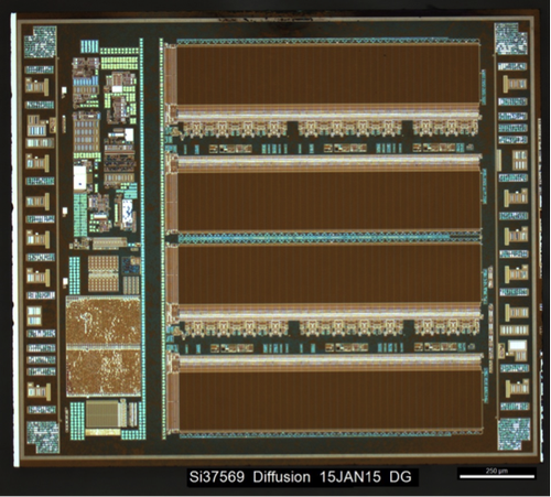
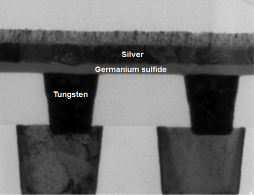
Adesto uses a conductive bridge technology for their RM24EP128KS, one-transistor one-resistor (1T1R) CBRAM product, and this is based on a silver/germanium sulfide/tungsten memory cell as shown in below. CBRAM relies on the formation of a conductive filament in a solid electrolyte (set) or its rupture (erase) due to an applied bias voltage. An oxidizable electrode such as silver or copper provides a source of metal ions that form conductive filaments in an insulating electrolyte. Adesto uses a silver anode for the ion reservoir, germanium sulfide chalcogenide glass as the electrolyte, and an inert tungsten cathode.
Click here for larger image
A positive bias (set) applied to the silver anode causes silver ions to migrate into the germanium sulfide layer, creating conductive filaments to the bottom tungsten cathode (conductive bridge). A negative bias (erase) reverses this process.


 留言列表
留言列表